Design World

  • Home
  • Technologies
    • 3D CAD
    • Electronics • electrical
    • Fastening & Joining
    • Factory automation
    • Linear Motion
    • Motion Control
    • Test & Measurement
    • 传感器
    • 流体动力
  • Learn
    • Ebooks / Tech Tips
    • Engineering Week
    • Future of Design Engineering
    • MC² Motion Control Classrooms
    • Podcasts
    • Videos
    • Webinars
  • LEAP AWARDS
  • 领导
    • 2022 Voting
    • 2021 Winners
  • Design Guide Library
  • Resources
    • 3D Cad Models
      • PARTsolutions
      • TraceParts
    • Digital Issues
      • Design World
      • EE World
    • Women in Engineering
  • Supplier Listings

New Theory Could Lead to New Generation of Energy Friendly Optoelectronics

ByQueen's University Belfast|August 22, 2016

Share

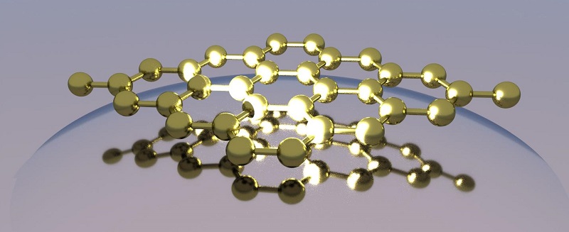
德维克的透明度e at the 2-D limit can be tuned using an electric bias, where different type of optical processes that simply define the way we see objects can be modify externally. This gives the control on properties that until very recently were not thought to be manipulated arbitrarily. Image credit: Queen’s University Belfast

Researchers at Queen’s University Belfast and ETH Zurich, Switzerland, have created a new theoretical framework which could help physicists and device engineers design better optoelectronics, leading to less heat generation and power consumption in electronic devices which source, detect, and control light.

Speaking about the research, which enables scientists and engineers to quantify how transparent a 2D material is to an electrostatic field, Dr Elton Santos from the Atomistic Simulation Research Centre at Queen’s, said: “In our paper we have developed a theoretical framework that predicts and quantifies the degree of ‘transparency’ up to the limit of one-atom-thick, 2D materials, to an electrostatic field.

“Imagine we can change the transparency of a material just using an electric bias, e.g. get darker or brighter at will. What kind of implications would this have, for instance, in mobile phone technologies? This was the first question we asked ourselves. We realised that this would allow the microscopic control over the distribution of charged carriers in a bulk semiconductor (e.g. traditional Si microchips) in a nonlinear manner. This will help physicists and device engineers to design better quantum capacitors, an array of subatomic power storage components capable to keep high energy densities, for instance, in batteries, and vertical transistors, leading to next-generation optoelectronics with lower power consumption and dissipation of heat (cold devices), and better performance. In other words, smarter smart phones.”

Explaining how the theory could have important implications for future work in the area, Santos said, “Our current model simply considers an interface formed between a layer of 2D material and a bulk semiconductor. In principle, our approach can be readily extended to a stack of multiple 2D materials, or namely, van der Waals heterostructures recently fabricated. This will allow us to design and predict the behaviour of these cutting-edge devices in prior to actual fabrication, which will significantly facilitate developments for a variety of applications. We will have an in silico search for the right combination of different 2D crystals while reducing the need for expensive lab work and test trials.”


Filed Under:Capacitors,Materials • advanced


Related ArticlesRead More >

Self-lubricating and wear-resistant: igus bar stock for food, continuous operation and high media resistance
Minnesota Rubber and Plastics announces plans for new Innovation Center
The importance of resin selection
EXE014 - Image 1
Composite materials help place Italian race team in pole position

DESIGN GUIDE LIBRARY

“motion

Enews Sign Up

Motion Control Classroom

Design World Digital Edition

cover

Browse the most current issueof Design World and back issues in an easy to use high quality format. Clip, share and download with the leading design engineering magazine today.

EDABoard the Forum for Electronics

Top global problem solving EE forum covering Microcontrollers, DSP, Networking, Analog and Digital Design, RF, Power Electronics, PCB Routing and much more

EDABoard: Forum for electronics

Sponsored Content

  • Global supply needs drive increased manufacturing footprint development
  • How to Increase Rotational Capacity for a Retaining Ring
  • Cordis high resolution electronic proportional pressure controls
  • WAGO’s custom designed interface wiring system making industrial applications easier
  • 10 Reasons to Specify Valve Manifolds
  • Case study: How a 3D-printed tool saved thousands of hours and dollars

Design World Podcasts

May 17, 2022
Another view on additive and the aerospace industry
See More >
Engineering Exchange

The Engineering Exchange is a global educational networking community for engineers.

Connect, share, and learn today »

Design World
  • 广告
  • About us
  • Contact
  • Manage your Design World Subscription
  • Subscribe
  • Design World Digital Network
  • Engineering White Papers
  • LEAP AWARDS

Copyright © 2022 WTWH Media LLC. All Rights Reserved. The material on this site may not be reproduced, distributed, transmitted, cached or otherwise used, except with the prior written permission of WTWH Media
Privacy Policy|广告|About Us

Search Design World

  • Home
  • Technologies
    • 3D CAD
    • Electronics • electrical
    • Fastening & Joining
    • Factory automation
    • Linear Motion
    • Motion Control
    • Test & Measurement
    • 传感器
    • 流体动力
  • Learn
    • Ebooks / Tech Tips
    • Engineering Week
    • Future of Design Engineering
    • MC² Motion Control Classrooms
    • Podcasts
    • Videos
    • Webinars
  • LEAP AWARDS
  • 领导
    • 2022 Voting
    • 2021 Winners
  • Design Guide Library
  • Resources
    • 3D Cad Models
      • PARTsolutions
      • TraceParts
    • Digital Issues
      • Design World
      • EE World
    • Women in Engineering
  • Supplier Listings
We use cookies to personalize content and ads, to provide social media features and to analyze our traffic. We also share information about your use of our site with our social media, advertising and analytics partners who may combine it with other information that you’ve provided to them or that they’ve collected from your use of their services. You consent to our cookies if you continue to use this website. OkNoRead more