

 In the future, mobile devices will be able to quickly and realistically detect their surroundings in three dimensions (3D). When they do, it will be thanks to the 3D image sensor chips from Infineon Technologies AG and pmdtechnologies gmbh. REAL3 will enable extremely realistic virtual and augmented reality game experiences that involve the interaction of the gamer’s own hands and his living environment within the game via head-mounted devices. Other image sensor chip applications include the spatial measurement of rooms and objects, indoor navigation and the implementation of special photo effects.
英飞凌和pmd showcasing the latest 3D image sensor chip of the REAL3 family at the Consumer Electronics Show (CES) 2016 in Las Vegas. Compared to the previous version, the optical sensitivity as well as the power consumption of the new 3D image sensors has been improved. Moreover, the built-in electronics take up little space. The chips make it possible for cell phones to operate mini-camera systems that can measure 3D depth data.
Using microlenses for high sensitivity
The camera’s range and measurement accuracy depend on two factors: on the intensity of the emitted and reflected infrared light, and to a significant extent on the pixel sensitivity of the 3D image sensor chip. The optical pixel sensitivity of the new 3D image sensor chips are now double that of the previous version. This means that their measurement quality is just as good, while at the same time working with only half of the emitted light output. Thus, manufacturers of camera systems for mobile devices can not only provide the infrared lighting more cost-effectively, but the camera’s system power consumption is almost halved.
The improved optical pixel sensitivity is the result of applying one microlens to each of the pixels of the 3D image sensor chip. Consequently most of the incident light is directed to a pixel’s sensitive surface, so virtually no light energy is lost to the inactive areas anymore.
Optimized form factor: half the sensor size
3 d图像传感器芯片是展示了CES were specifically designed for mobile devices, where most applications only need a resolution of 38,000 pixels. The previous 100,000-pixel matrix was accordingly scaled down, and other functional blocks, such as the analog/digital converter for the chip area and performance range were optimized. Thus, the system costs are lower: the sensor chip area is almost halved, and, because of the lower resolution, smaller and less expensive optical lenses can be used.
New 3D image sensor chips with 19,000; 38,000 and 100,000 pixels
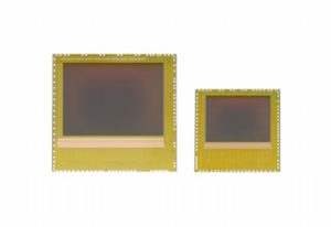
The three new REAL3 3D image sensor chips are all equipped with microlenses and have almost the same level of optical performance and functionality. They differ only in their resolutions: the IRS1125C works with 352 x 288 pixels, the IRS1645C with 224 x 172 pixels and the IRS1615C with 160 x 120 pixels. In this respect, the IRS1645C and IRS1615C are produced on half the chip area of the IRS1125C.
Google’s “Project Tango” using Infineon’s IRS1645C 3D image sensor chip
The IRS1645C is particularly suitable for use in mobile devices. Infineon and pmdtechnologies are joint partners in Google’s “Project Tango”. With “Tango”, cell phones and tablets are equipped with a special optical sensor system for 3D perception, which includes a 3D camera with Infineon’s IRS1645C 3D image sensor chip. Applications are augmented reality, indoor navigation and three-dimensional measurement. The complete 3D camera for Google “Tango” – consisting of IRS1645C and an active infrared laser illumination – is housed in an area of approximately 10 mm x 20 mm. With a range up to 4 meters (13 feet), a measuring accuracy of 1 percent of the distance and a frame rate of 5 fps (frames per second), the 3D camera subsystem consumes less than 300 mW in active mode.
Time-of-Flight Principle (ToF)
The 3D image sensor chips operate with infrared light and use the time-of-flight (ToF) measuring principle: For each of its pixels, the 3D image sensor chip measures the time the infrared light takes to travel from the camera to the object and back again. At the same time, each of the pixels also detects the brightness value of the objects.
The IRS1125C will be available in volume as of first quarter of 2016. The start of production for the smaller IRS1645C and IRS1615C is planned for the second quarter of 2016. All three types are exclusively delivered as a bare die to allow maximum design flexibility while minimizing system costs.
About the cooperation between Infineon and pmdtechnologies
Infineon co-developed the REAL3 3D image sensor chip with pmdtechnologies gmbh from Siegen, Germany. Both companies are providing the technical support for customers jointly. pmdtechnologies’ contribution to the new chip family is the ToF pixel matrix. Infineon contributes all functional blocks for the system-on-chip (SoC) integration and developed the manufacturing process. The 3D image sensor chips are produced in Infineon’s Dresden plant with a CMOS process optimized for ToF using microlens technology.
Infineon and pmdtechnologies at the CES 2016
At the Consumer Electronics Show 2016 in Las Vegas (January 6-9, 2016), Infineon and pmd will be presenting the performance of the 3D image sensors in demonstrations and concept designs for cell phone and head-mounted device applications. Queries on meeting alignment at[email protected]
进一步在英飞凌的3 d技术信息mage sensor chips is available at www.infineon.com/3d-imaging. Information about prototype cameras and the pmd technology is available at www.pmdtec.com
Infineon
PMD Technology
infineon.com
pmdtec.com
Filed Under:Sensor Tips,Virtual reality


