

S2C Inc.是SOC / ASIC快速原型解决方案提供商,宣布其Protobridge™AXI现在支持具有柔性总线宽度的AXI-4协议,以提高数据传输速度。Protobridge Axi是一个FPGA加速的验证工具,使设计人员能够从计算机读取和写入基于AXI的设计,映射到基于FPGA的原型。通过利用丰富的C子程序调用,Protobridge AXI用户可以轻松实现算法验证,块级原型设计,全芯片仿真加速度,转角案例测试和早期SoC软件开发。
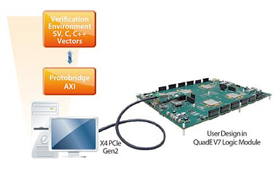
ProtoBridge AXI consists of a computer software component and a FPGA design component. The computer software component contains Linux/Windows drivers and a set of C-API/DPI routines to perform AXI transactions. The FPGA design component contains a PCIe, an interconnection module and AXI transactors to be instantiated in users’ design-under-test (DUT). With these enhanced product features, users can read and write at speeds of up to 500 megabytes per second through the PCIe interface, connect 8 Master devices and 8 Slave devices on the AXI bus, and take advantage of the patent pending Shared Memory technology that link the FPGA prototype with third party design tools.
“FPGA-based prototypes today are predominantly used at late design stages such as system validations and software developments. Our customers have requested us to provide solutions for earlier design stages.” said Toshio Nakama, Chief Executive Officer of S2C. “S2C’s ProtoBridge AXI software has already been deployed at a number of S2C customer sites and delivered great results. We are pleased to release the updated version of ProtoBridge AXI which facilitates designers to maximize the benefits of FPGA-based prototypes early in the design project for algorithm validation, IP design, simulation accelerations and corner case testing.”
“We at Fullhan Microelectronics are happy to use ProtoBridge AXI in our design project”, said Gao Houxin, R & D Director of Fullhan Microelectronics. “Fullhan is a worldwide leading supplier of video surveillance chips and system solutions. High-performance H.264 Video Encoder is one of our major products, and our design challenge is the short market window. The video streams to be tested on the design are huge in size, and we don’t want to put all that testing work late in the FPGA prototyping stage. We utilized ProtoBridge AXI’s C-API functions and successfully transferred the video streams to and from the design blocks mapped on FPGAs to finish testing early in the block design stage, and that shortened our H.264 project design cycle”.
原型化平台支持
S2C的Protobridge AXI通过通过S2C 4-Lane PCIe Gen2 GTX模块连接S2C的V7和K7 Tai逻辑模块系列。V7 Tai逻辑模块可以在单板上原型SOC / ASIC设计高达8000万个ASIC门,可以堆叠或铺设多个逻辑模块,以满足更高的栅极容量要求。有关Protobridge Axi及其支持的硬件的更多信息,请访问S2C网站上的Protobridge Axi产品页面。
S2C解决方案使设计人员能够快速创建可以在实时速度运行或接近实时运行的SOC原型,从而实现全面的硬件验证和早期软件开发。S2C的灵活,可扩展和可重复使用的硬件架构与基于事务的链接到系统模拟,使S2C解决方案成为从算法探索,IP设计,系统集成到兼容性测试的主要设计阶段的理想常见平台。
S2C Inc.
www.s2cinc.com
帖子S2C ProtoBridge AXI Expands FPGA-Based Prototype Usage首先出现了FPGA Tips.
Filed Under:FPGA Tips


