

The discovery of lead in Flint, Michigan’s drinking water drew renewed attention to the health risks posed by the metal. Now researchers at the University of Houston have created an inexpensive system using a smartphone and a lens made with an inkjet printer that can detect lead in tap water at levels commonly accepted as dangerous.
The system builds upon earlier work by Wei-Chuan Shih, associate professor of electrical & computer engineering, and members of his lab, including the discovery of an inexpensive elastomer lens that can convert a basic smartphone into a microscope.
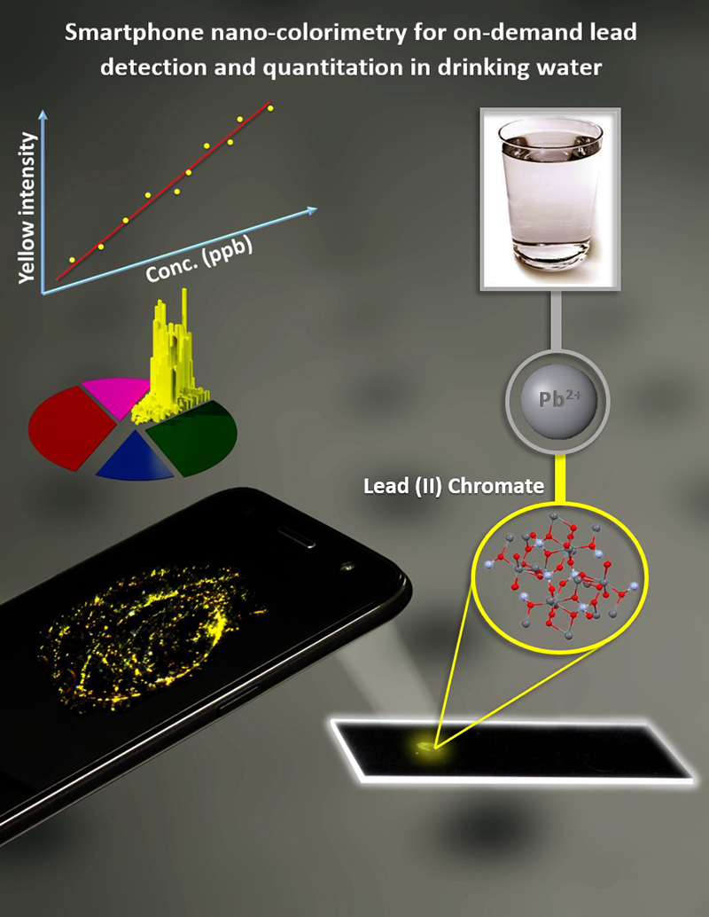
The latest discovery, described in the journal Analytical Chemistry, combines nano-colorimetry with dark-field microscopy, integrated into the smartphone microscope platform to detect levels of lead below the safety threshold set by the Environmental Protection Agency.
“Smartphone nano-colorimetry is rapid, low-cost, and has the potential to enable individual citizens to examine (lead) content in drinking water on-demand in virtually any environmental setting,” the researchers wrote.
Even small amounts of lead can cause serious health problems, with young children especially vulnerable to neurological damage. EPA standards require lead levels in drinking water to be below 15 parts per billion, and Shih said currently available consumer test kits aren’t sensitive enough to accurately detect lead at that level.
By using an inexpensive smartphone equipped with an inkjet-printed lens and using the dark-field imaging mode, researchers were able to produce a system that was both portable and easy to operate, as well as able to detect lead concentrations at 5 parts per billion in tap water. The sensitivity reached 1.37 parts per billion in deionized water.
Shih and his students last yearpublishedan open-source dataset in Biomedical Optics Express, explaining how to convert a smartphone equipped with the elastomer lens into a microscope capable of fluorescence microscopy. That paper has been the journal’s most frequently downloaded paper since its publication.
最新的应用程序包含颜色分析to detect nanoscale lead particles. In addition to Shih, researchers on the project include first author Hoang Nguyen and Yulung Sung, Kelly O’Shaughnessy and Xiaonan Shan, all with the UHDepartment of Electrical & Computer Engineering. (O’Shaughnessy was a summer intern from the University of Cincinnati under the National Science Foundation’s Research Experiences for Undergraduates program.)
Applying the dataset published in 2017, the researchers built a self-contained smartphone microscope that can operate in both fluorescence and dark-field imaging modes and paired it with an inexpensive Lumina 640 smartphone with an 8-megapixel camera. They spiked tap water with varying amounts of lead, ranging from 1.37 parts per billion to 175 parts per billion. They then added chromate ions, which react with the lead to form lead chromate nanoparticles; the nanoparticles can be detected by combining colorimetric analysis and microscopy.
The analysis measured both the intensity detected from the nanoparticles, correlating that to the lead concentration, and verified that the reaction was spurred by the presence of lead.
The mixture was transferred to a polydimethylsiloxane slab attached to a glass slide; after it dried, deionized water was used to rinse off the chromate compound and the remaining sediment was imaged for analysis.
The microscopy imaging capability proved essential, Shih said, because the quantity of sediment was too small to be imaged with an unassisted smartphone camera, making it impossible to detect relatively low levels of lead.
Building upon the smartphone microscope platform to create a useful consumer product was key, Shih said. “We wanted to be sure we could do something that would be useful from the standpoint of detecting lead at the EPA standard,” he said.
The researchers built a self-contained smartphone microscope that can operate in both fluorescence and dark-field imaging modes and paired it with an inexpensive Lumina 640 smartphone with an 8-megapixel camera. Credit University of Houston
Filed Under:Test + measurement • test equipment


